REATISS Unlock patent value
Services
 Product Analysis
This analysis can be helpful for a customer in a different ways:
- Compare competitor product with similar products within a customer products
- Find the outstanding features of competitor product
- Improve the competitive position on the market
- Benchmark against future technology plans
REATISS provides several fundamental types (levels) of analytical reports to gain a wider understanding of the package and silicon processing techniques utilized by the competitive devices.
It serves for decision making regarding further analysis steps.
Report contents:- Package photos, marking
- Package X-Ray
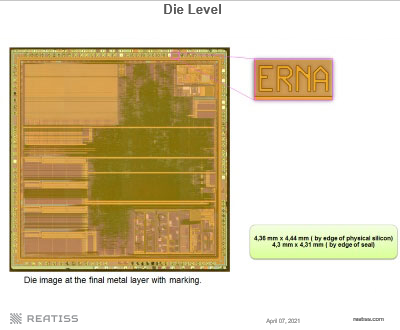
- Photo of die at top metal level
- Photo of die markings
- Die and package dimensions
For this purposes the die is de-processed down to Metal1 or Diffusion level. The deliverables can be used for comparison with the customer own product and drawing conclusions regarding the die area utilization.
Report contents:- Package photos
- Package X-Ray
- Photo of die at top metal level
- Package X-Ray and die combined image
- Die and package dimensions
- Photo of die markings
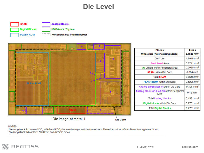
- Photo of die at metal 1 / diffusion level
- Boxing of the different blocks
- Table account for the total die size per block (Flash, RAM, Analog blocks, Digital, Core area, total die)
-
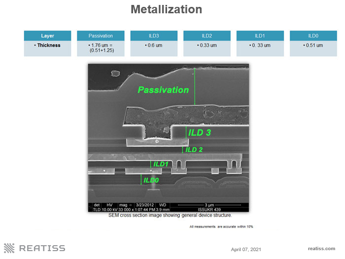
Technology analysis
- # of metals, metallization materials
- Vertical dimension measurements
- Cross section images showing general device structure
- Gate length measurements
-
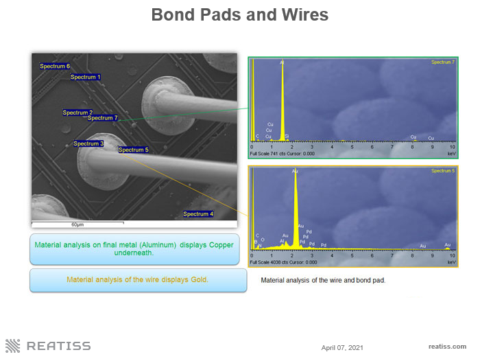
Bond pads
- Image of die fragment and bond pads
- Bond pad blowup image
- # of pads, pads bonded out
- Pad measurements
-
Standard cell analysis
- High-resolution top-down image in the sea of gates at M1 or poly
- Standard cell size measurements
- Cross section of MOS devices, gate length measurements
-
Functional analysis
- Major functional block identification
- Size measurements for major blocks
- High resolution images of major blocks
-
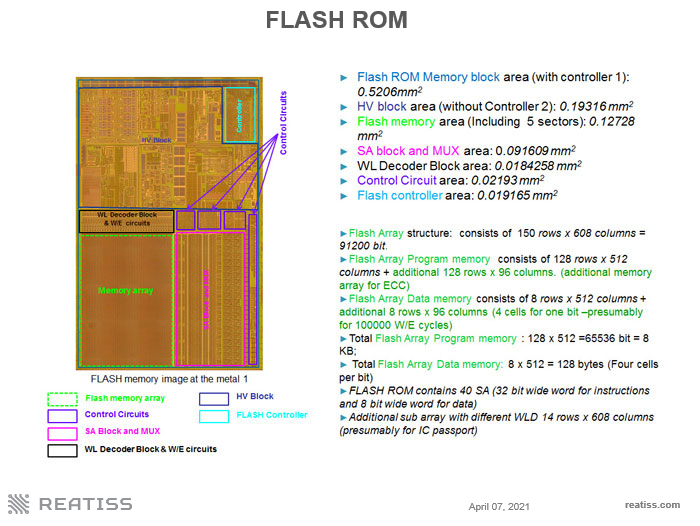
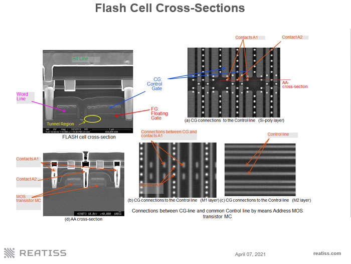
Memory analysis (Flash, SRAM)
- High-level structure
- High-resolution top-down bit cell image at M1 or poly
- Bit cell size measurements
- Efficiency calculation
- Flash cross section, feature size measurements
- Digital/analog schematics organized in a hierarchical manner (I/O Buffers, SRAM, FLASH, PLL, ADC, focused extraction of sea of gates etc.)
- Signal tracing
- Transistor-level details
- Access to a high resolution layout image data base (focused areas/full die)
The results received through a package cross sections, material analysis, and physical dimension measurements. A customer may define particular areas of interest in order to perform benchmarking with own product in a most efficient way.
Standard report contents:- Package photos
- Package X-Ray with construction dimensions.
- Die top metal: die photo, dimensions, marking;
- Bond pad photos with dimensions; wire measurements.
- Inspect die edge for chipping/peeling.
- Package cross-sections (through the leadframe, terminals, die): material analysis, construction detailed photos, measurements.
As a part of service, REATISS provides constant support and response to engineering requests for clarification of the data and additional information on a competitive die/package.