REATISS Unlock patent value
Services
 Process Analysis
REATISS provides process analysis of semiconductor devices which gives understanding of structure of integrated circuit and packaging. This analysis could improve technology steps, material choice, yield efficiency, and uncover evidences of process patents infringements.
REATISS capabilities allow reverse engineering on following types of the devices: CMOS and BiCMOS ICs, MEMS, optic sensors, high frequency ICs, different types of memory, etc.
The results are provided in a form of the report including following chapters:
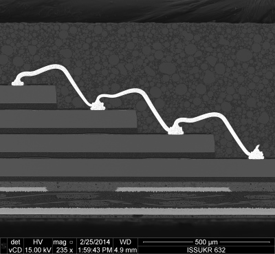
Die and package analysis
Optical image of package top and bottom, top-down package X-Ray image, optical die image at the final metal level, panoramic package cross section, in depth bond pad analysis including Energy Dispersive X-Ray Spectroscopy (EDX) mapping. Measurements of general feature sizes.
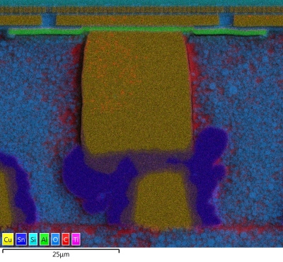
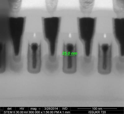
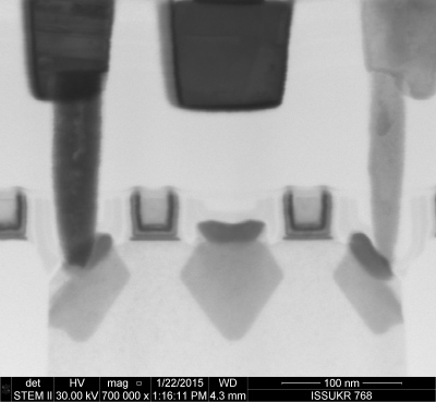
Process analysis
SEM/STEM images of general device structure, metal lines, contacts, vias, MOS gates, and other specific features. Energy Dispersive X-Ray Spectroscopy (EDX) mapping of STEM section of metal lines, dielectrics, silicides, barrier layers. Measurements of general feature sizes.
CA report helps to understand
- Construction of package and die/dice connection
- Material of wires, bumps or pillars
- Number of metal layers
- Material of metal interconnect layer
- Structure of IC features
- Minimum printed gate length
On customer request REATISS can perform focused process analysis, where the specific IC or package features are analyzed in more detail. This analysis can include delayering of selected die areas, high-resolution optical and SEM imaging, and creating multi-layer images database.
Typical cycle time for CA is 2-3 weeks for Package Analysis and 4-6 weeks for full Process Analysis. Typical CA report could be found here:
Process Report Example